Beginner Tutorial to KiCAD
Installation
Download and install KiCAD from https://www.kicad.org.
Schematic
Open KiCAD and start a new project. Once the project is created, open the schematic of the project. Here is where you’ll draw the electronics schematic for your project.
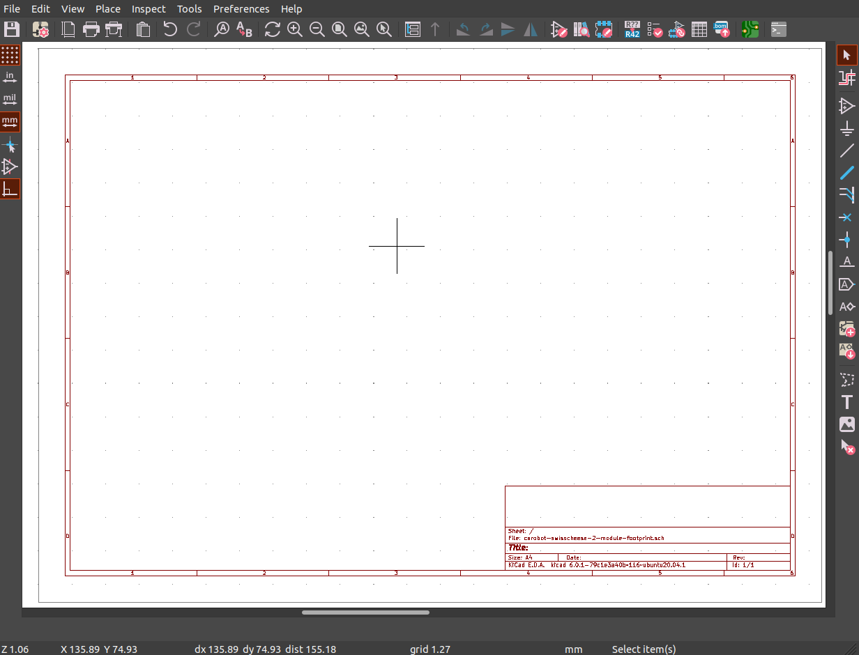
In this tutorial, we are going to create a simple circuit that consists of a NPN transistor driving a LED.
First, let’s add some component symbols to your schematic.
Click on the Add a symbol icon ![]() or A on your keyboard. Filter for R for the resistor and select the standard resistor symbol.
or A on your keyboard. Filter for R for the resistor and select the standard resistor symbol.
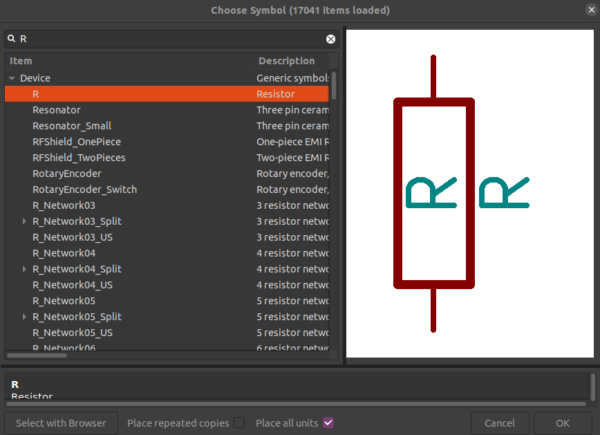
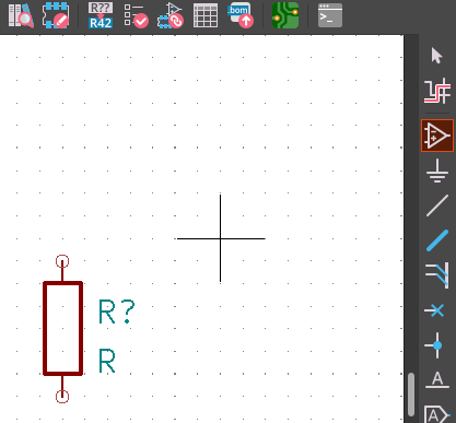
Click OK then place it onto your schematic.
You can zoom in to your schematic using your mouse wheel or the zoom in and zoom out button.
![]()
Repeat adding a second resistor and a LED in the schematic. Since most resistors and LEDs only have two leads, we can use the standard component symbol.
Tips: You can duplicate a symbol by highlighting it and press Ctrl + D on your keyboard.
Tips: When you are in symbol adding mode, you can just left-click anywhere on the schematic and not have to click the Add a symbol button to add the next symbol.
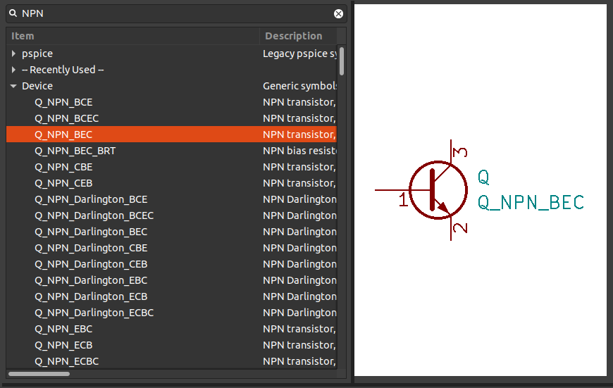
Next, we'll add a NPN transistor to our circuit. NPN transistors have several configurations depending on the pin arrangement. For our design, we'll be using a BC846/7/8 series transistor (datasheet). As per the datasheet, the pins configuration is pin 1 = Base, pin 2 = Emitter, pin 3 = Collector. Therefore, we'll select the Q_NPN_BEC symbol.
Click OK then place it onto your schematic.
Next, we'll add a 3-pin connector so our circuit can be connected to other electronic devices using jumper cables or wires. There are various 1x3 connector symbols that you can use by one we prefer is the Conn_01x03 symbol.
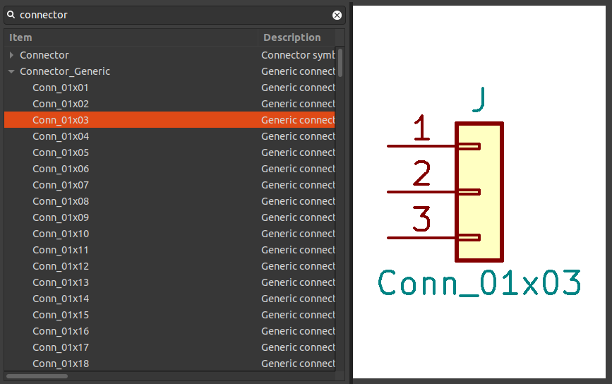
Click OK then place it onto your schematic.
Before we start connecting all the symbols, we'll add some power symbols to identify the Vcc and GND of our circuit. Click on the Add a power port icon ![]() or P on your keyboard. Filter for VCC and add two VCC symbols. Next, Filter for GND and add two GND symbols.
or P on your keyboard. Filter for VCC and add two VCC symbols. Next, Filter for GND and add two GND symbols.
Rearrange the symbols so they are similar to the diagram below.
Tips: Use Esc on your keyboard to exit the current edit mode or cancel any edit command.
Tips: Rotate a symbol by right-click on the symbol and select Rotate Counterclockwise or R.
Tips: Move a symbol by clicking on it once then click and drag. Alternatively, you can right-click on the symbol and select Move or use the keyboard shortcut M.
Tips: Flip a symbol by right-click on the symbol and select Mirror Vertically Y or Mirror Horizontally X.
Tips: Rotate a symbol by right-click on the symbol and select Rotate Counterclockwise or R.

Lastly, we'll connect all the components together. Click on the Add a wire icon ![]() or W on your keyboard.
or W on your keyboard.
At each component, unconnected nodes are identified by a small circle at each lead.

Connect all the nodes using the wire tool to complete the circuit.

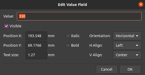
Our circuit is now completed but we still need to add component value for the resistors. Right-click on each of the resistor and select Edit Value or left-click on over each of the resistors then press V on your keyboard.
Once drafting of the circuit is done, we'll move on to adding annotations to the circuit components, such as R1, D1, etc. Go to Tools > Annotate Schematic to open the annotation menu.
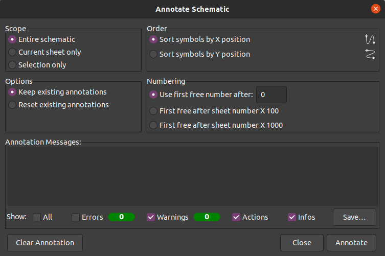
You can keep all the default settings then click Annotate then Close the menu. All the components in the schematic should now have numberings.

The last step before we can move on to working with the PCB layout is assigning a footprint to each component symbol in the schematic. Assignment of a footprint will require us knowing or having a very good idea of which physical component we are going to use in our circuit because electronics components such as a resistor, LED, transistor come in different shapes and sizes. For some of the common components, you might not need to know the exact parts number at this point, but for application-specific components such as sensors, you might want the parts number handy so you won't choose the wrong footprint for your design. Go to Tools > Assign Footprints.
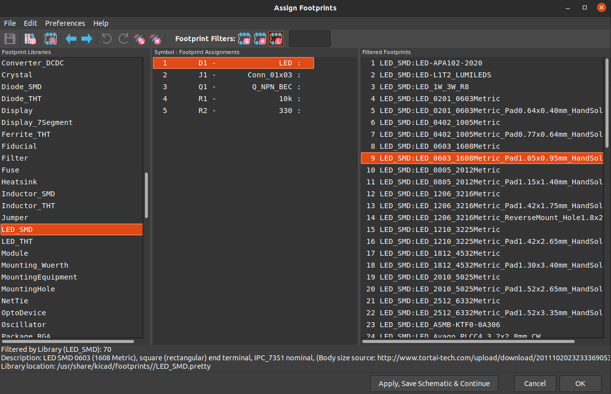
In the Assign Footprints window, you'll see three columns. The column on the left is where you'll find all your Footprint Libraries. The centre column is a list of all the components in your schematic. The column on the right is a list of footprints from the library you select that you can assign to the components in the centre column.
First, we'll assign a surface mount LED with a size specification of 0603 to the component D1. Scroll down to the LED_SMD library then select component D1 then double-click on the LED_SMD:LED_0603...HandSolder footprint. We are choosing the hand solder version of the footprint because we'll most likely hand solder on the SMD component during prototyping.
Tips You can right-click on the footprint to see a preview of it.
Repeat the process to assign footprints to the components as per the following table:
| Symbol | Footprint Library | Footprint |
|---|---|---|
| D1 | LED_SMD | LED_0603...HandSolder |
| J1 | Connector_JST | JST_PH_B3B-PH-SM4... |
| Q1 | Package_TO_SOT_SMD | SOT-23 |
| R1 | Resistor_SMD | R_0603...HandSolder |
| R2 | Resistor_SMD | R_0603...HandSolder |
The footprint assignment list should look like this after you are done.
Click Apply, Save Schematic & Continue then click OK to close the window. Now we can move on to the board layout.
Board Layout
After everything from the schematic is set, we are ready for the board layout. Open the PCB file in your project or click on the PCB editor icon  from the Schematic Editor.
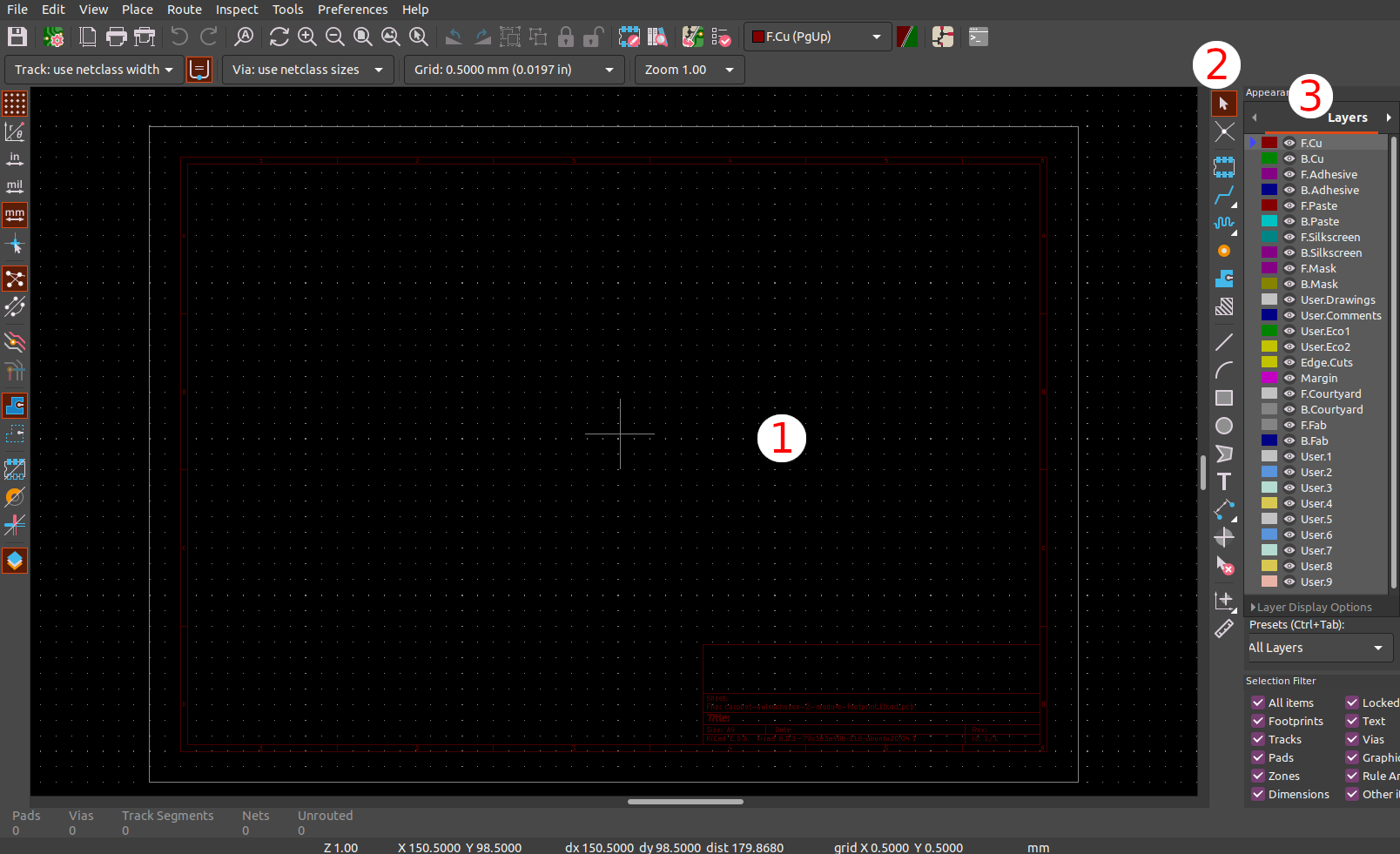
The PCB editor might seem very intimidating at first but there are only a few areas that you have to worry about for simple PCB design. There is the:
- (1) The draft area - this is where you will place the component and draw your PCB.
- (2) The tool column - this is where you can find the majority of the tools that you'll need.
- (3) The Layers panel - this is where you can toggle the visibility on/off for various layers of your PCB design.
The first thing that we'll need to do is populate the drawing with the components from the schematics. Go to Tools > Update PCB from Schematic or press F8 on your keyboard. After you open the Update PCB from Schematic window, click Update PCB then Close.
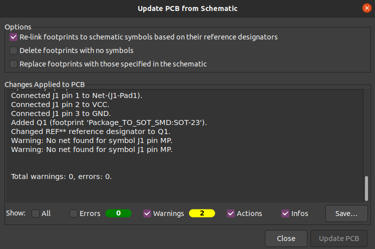
NOTE: For this tutorial, you can ignore the warnings as it is just due to the JST connector mounting pad.
Once you click Close, the components will appear on the drawing. Click anyway on the drawing to place the components.

Zoom in a bit so you can see the components more clearly. What you should see now are component footprints with airwires (white) connecting them. The airwires are not actual wires and are just there to show you which solder pads should be connected as per the schematic. When designing a circuit board, the general rule is to minimize airwire from interacting to make trace drawing easier.
Let's use the same technique we used in the schematic editor to rearrange the components as per the figure below (or any design that you want). NOTE Do not flip the components! Flipping a component will cause it to go to the bottom/back layer.
TIPS: You can turn visibility off with some of the layers to reduce the amount of text on the screen. The F.Fab is safe to be turned off for the time being.
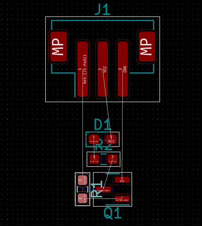
If you want, you can change the Grid setting to make the snap to grid pattern more fine or coarse.
![]()
Next, we'll start connecting the pads by drawing traces between them. But before we can draw those traces, we need to know what trace width to use. To figure out what trace width to use, KiCAD is packaged with a PCB calculator. Open up the PCB calculator. (It is a separate application installed along with KiCAD so you might need to find it from the Start Menu or in the folder where KiCAD is installed.) Go to the Track Width tab and insert parameters such as Current, Temperature rise, Conductor length into the calculator. Afterward, the calculator should provide you with details regarding External Layer Traces and Internal Layer Traces. For this project, we'll only be dealing with external traces.
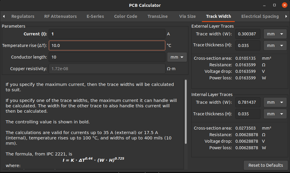
From the example above, we used 1A as the trace current, 10°C as the maximum temperature rise, and 10mm as the trace length. The result from the calculator is to use 0.3mm trace width when using 0.035mm (1oz copper) thickness. To be on the safe side, we'll use 0.4mm trace width for our project.
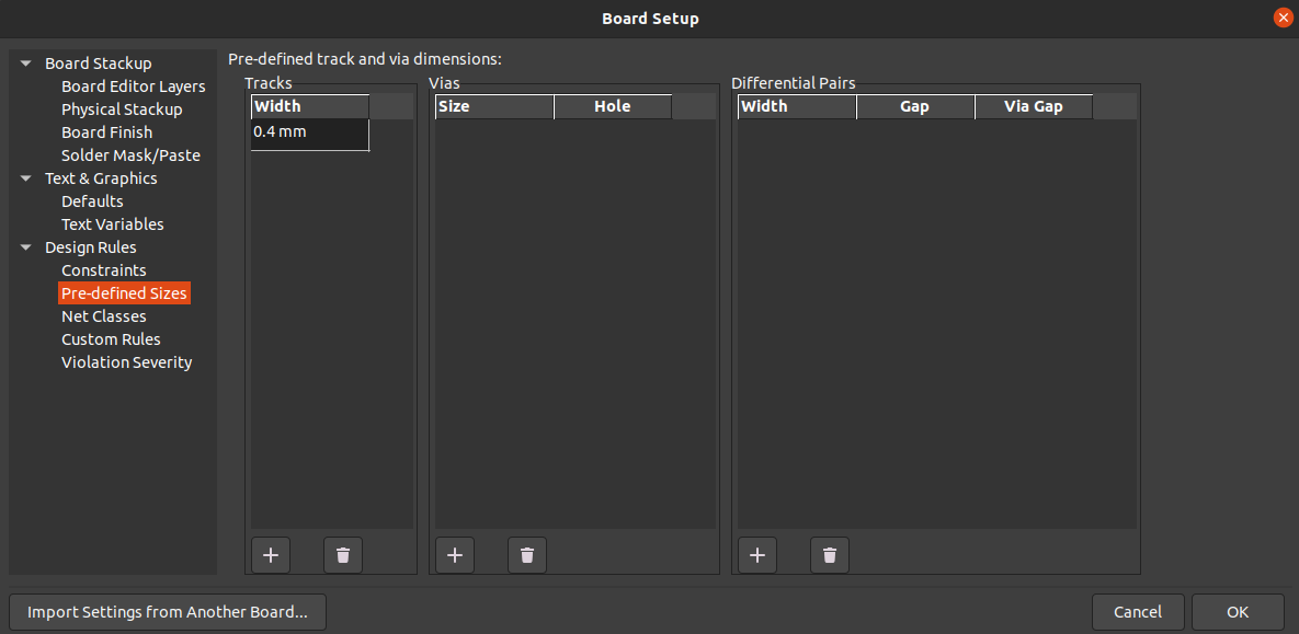
Now, click on the Track:use netclass width selector and select Edit Pre-defined Size.
![]()
We'll keep it simple by manually defining the trace size instead of defining a netclass for trace size. Click the "+" symbol under Tracks and insert 0.4mm. Hit Enter on your keyboard then click OK.
Once the track size is set up, we'll select it in the track size menu.
![]()
Ensure you are drawing on the front / top copper layer by selecting F.Cu in the Layers Panel then start connecting the pad together by clicking on the Route icon or X on your keyboard. Use the airwire as a guide. If you make a mistake, right-click on the trace and select delete to remove the trace.
TIPS: As a general rule, avoid interaction of two copper edges that are less than 90°.
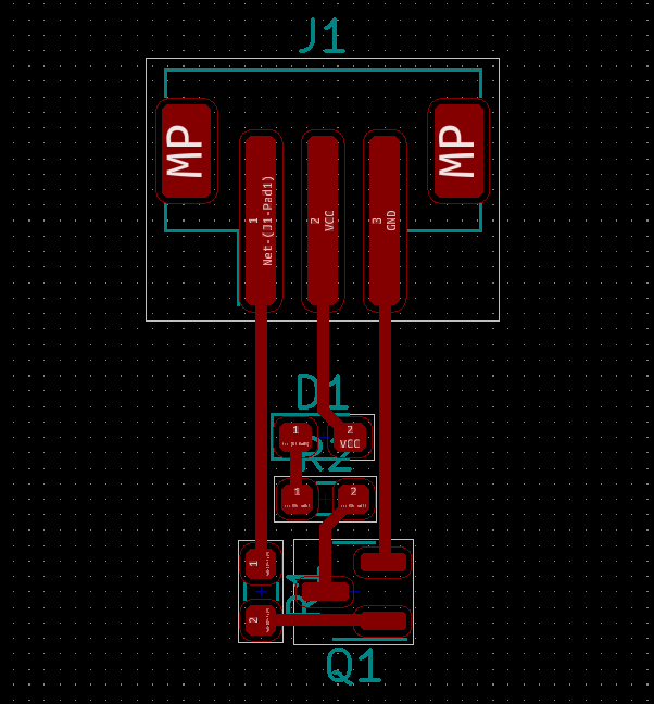
Once you routed all the airwires, your design should look something similar to the figure below.
Next, we'll define the physical outline of the PCB. Select the Edge.Cuts layer then using the line tool (Crtl + Shift + L) and/or arc tool (Crtl + Shift + A) to draw the outline.
![]()
Ensure the shape is a closed path. If mounting holes are required, use either the circle tool or a via.
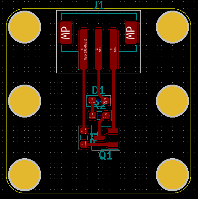
We designed our board to look something like the figure below.
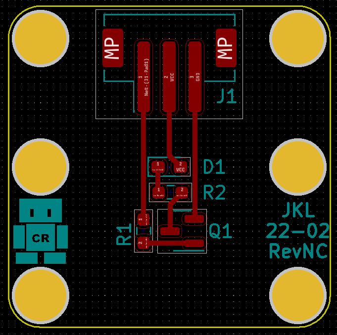
Lastly, let's arrange the silkscreen marking by selecting the F.Silkscreen layer and move the component reference around. We can also add some logos and graphics to customize the board. It is always a good idea to put the initial of the drafter, a date, and a revision to each board if space permits. Keep in mind that markings that are too small will not be legible depending on the capability of the fabrication house.
All done!
To have the PCB manufactured, consult the PCB manufacturer of your choice and follow their instruction on how to prepare the Gerber files.
NOTE This is a very simplified tutorial and a lot of KiCAD functions and PCB design concepts are not covered. For more details and reference materials on how to design PCB, you can refer to Getting Started with KiCAD from the KiCAD documentation or other resources you may find on the internet.
Other Resources
Altium, the developer of a paid commercial PCB design software also has some great resource on how to design PCB. https://resources.altium.com/pcb-layout