Design
High-Level Design
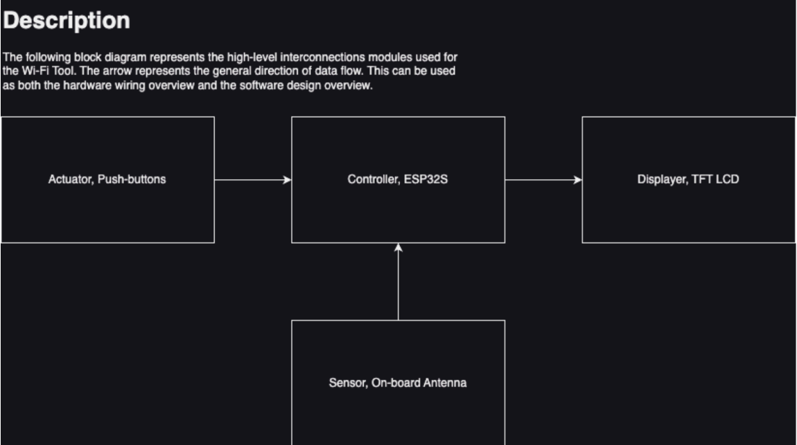
The design of Wifi Tool emphasizes modularity with iterative feature-rollouts. Data is collected via the antenna, processed by the ESP32 MCU, and displayed by the LCD. Control mechanisms such as interrupts and UI scrolling are implemented by pushbuttons switches respectively. The below functional diagram outlines the process-flow of the system.
Functional Block Diagram
It is advised for the readers to think about how to design the software augmentations in addition to the existing code base, and the above block diagram is a good entry point for thinking about the modularity of the design in an abstract view.
Detailed Design
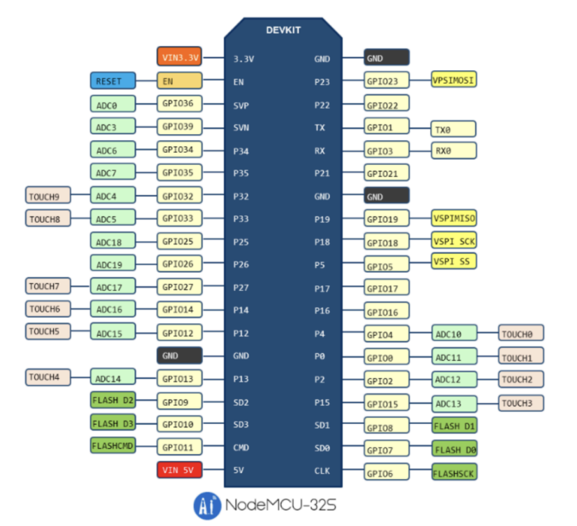
ESP32S - NodeMCU Edition
We need to be careful of working with ESP modules due to a variety of versions which may cause wiring confusion. The specific model to this project is the NodeMCU version, and the pin layout is illustrated below.
Note it supports both 3.3V and 5V input voltages.
The TFT LCD Wiring
Due to manufacturing variability, one may expect the LCD module to be different in terms of the pin-outs. The below table shows the connection established between the LCD and the ESP32 MCU.
| LCD Pin | Description | To ESP Pin |
|---|---|---|
| 1 – RST | Reset | GPIO 27 |
| 2 – CS | Chip Select | GPIO 5 |
| 3 – D/C | Data/Cmd | GPIO 32 |
| 4 – DIN | MOSI Slave | GPIO 23 |
| 5 – CLK | Clock | GPIO 18 |
| 6 – VCC | Power | 5V |
| 7 – BL | Backlight | 5V |
| 8 – GND | 0V | GND |
Button Wiring
There are a total of 5 push-buttons used for the user interface. Each button is wired with a pull-up resistor at 10k Ohms from the Vcc. The wiring diagram is shown below, and a 3.3uF capacitor is connected in parallel with the resistor for debounce purposes.

| PB | Description | To ESP Pin |
|---|---|---|
| 1 | Function | GPIO 15 |
| 2 | Go Back | GPIO 16 |
| 3 | Cursor Up | GPIO 17 |
| 4 | Cursor Down | GPIO 21 |
| 5 | Enter | GPIO 22 |